Sony and TSMC Are Exploring a Massive Chip Bet in Japan. Why a Planned $7 Billion Image Sensor Hub Matters Far Beyond Kumamoto
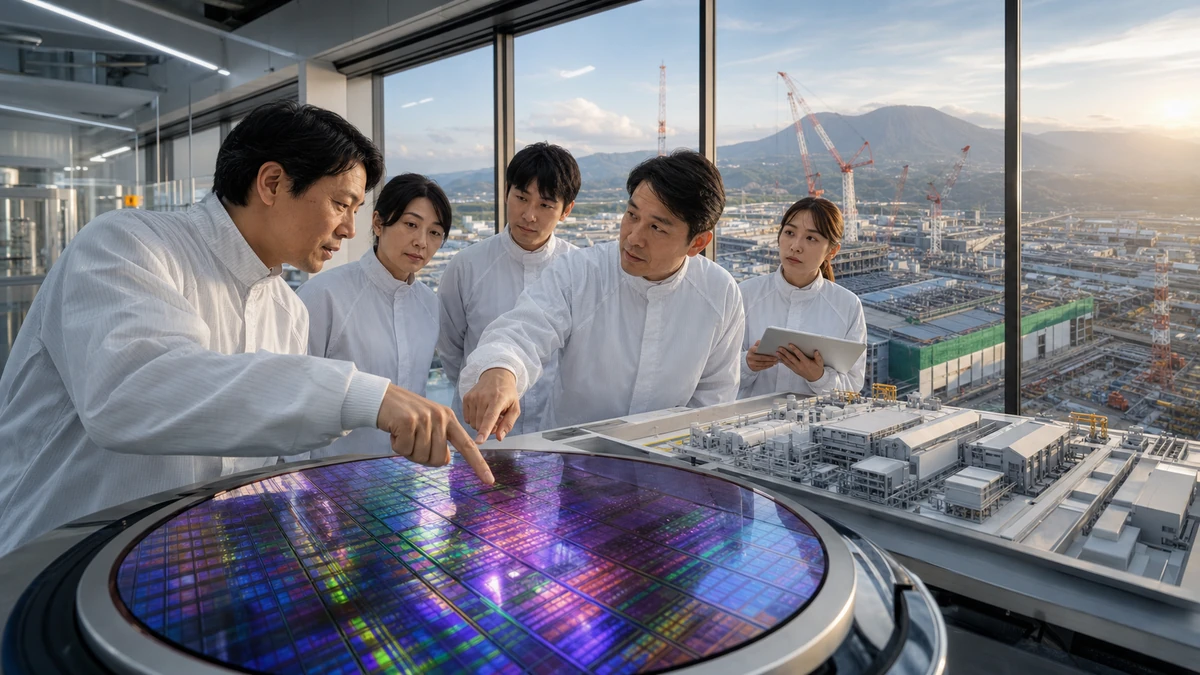
Image to help understand the article
A big semiconductor bet is taking shape in southern Japan
Sony and Taiwan Semiconductor Manufacturing Co., the world’s dominant contract chipmaker better known as TSMC, are reportedly weighing a joint investment of about 1 trillion yen, or roughly $7 billion, to build a next-generation image sensor production base in Kumamoto prefecture on Japan’s southern island of Kyushu. If the plan moves forward, it would rank as one of the most consequential semiconductor projects now under discussion in East Asia, not just because of its size, but because of what it says about the new geography of the global tech supply chain.
According to the Japanese business daily Nikkei, the companies are considering setting up a joint venture this year, with Sony holding about 60% and TSMC about 40%. The reported plan centers on Koshi, a city in Kumamoto where Sony Semiconductor already operates an image sensor plant. The goal under review is to begin mass production in 2029.
That is the hard information currently on the table: the proposed size of the investment, the likely ownership split, the location and the target production start date. But there is an important caveat. Neither Sony nor TSMC has publicly confirmed the project, and both companies reportedly declined to comment on the specifics of the Nikkei report. Japanese government subsidies, which often play a decisive role in projects of this scale, are also said to be under discussion, though no public details have been released on the amount, conditions or timing of any support.
Even in this still-unconfirmed phase, the reported talks are attracting attention because they bring together three forces reshaping the modern chip business: the race to secure strategic technologies, the push by governments to localize advanced manufacturing, and the growing recognition that no one company or country can shoulder the full cost of next-generation semiconductor production alone.
For American readers, it may help to think of this as more than a factory story. Image sensors are the components that let smartphones take photos, driver-assistance systems read the road, industrial robots “see” their surroundings, and surveillance, medical and augmented-reality devices turn light into digital data. In a world increasingly organized around cameras, automation and artificial intelligence, the humble image sensor has become one of the most important pieces of silicon most consumers rarely think about.
What image sensors are, and why they have become so strategic
An image sensor is the semiconductor that converts incoming light into an electronic signal, making digital photography and machine vision possible. If microprocessors are the brains of many devices, image sensors are increasingly their eyes. They sit behind the cameras in iPhones and Android phones, inside vehicle safety systems, in factory inspection equipment and in a widening range of consumer and industrial products.
Sony is the global leader in this field. For years, the Japanese company has supplied advanced image sensors to major smartphone makers and has held a powerful position in a business that blends precision manufacturing, optics, chip design and close customer relationships. In practical terms, that leadership means Sony is not simply making a commodity component. It is operating in a category that influences image quality, battery performance, low-light photography, machine perception and increasingly the performance of AI-enabled systems that rely on visual data.
That helps explain why the 1 trillion yen figure stands out. According to the Korean summary of the Japanese report, the amount is comparable to what Sony’s semiconductor unit would typically spend on capital investment over four years. In other words, one proposed joint manufacturing project could absorb an investment on the scale of several years of normal chip-equipment spending. That is a strong signal that Sony appears to view next-generation image sensors not as a routine capacity expansion, but as a core pillar of its long-term competitiveness.
In the semiconductor industry, those decisions are rarely about next quarter’s sales. Building and equipping a fab, or advanced chip production line, takes years and requires large upfront spending long before meaningful revenue arrives. A 2029 mass-production target suggests the companies, if they proceed, are thinking beyond today’s smartphone replacement cycle and toward the shape of the market later in the decade. That likely includes expectations for more advanced phone cameras, broader use of sensor-heavy AI systems, expansion in automotive vision and growing demand from industrial and infrastructure applications.
American audiences are already familiar with the strategic status of leading-edge chips through debates over Nvidia AI processors, Intel’s turnaround efforts and Washington’s CHIPS and Science Act. Image sensors belong to a different part of the semiconductor ecosystem, but the logic is similar: the technologies that control data capture, processing and manufacturing capacity increasingly carry geopolitical and economic weight.
Why Sony and TSMC would make an unusually powerful pairing
The proposed ownership split, with Sony at 60% and TSMC at 40%, offers a useful clue about how the project may be structured if it goes ahead. Sony’s majority stake suggests it would remain the central operating and commercial force, a logical outcome given its market leadership in image sensors and the fact that the project would be built around an existing Sony manufacturing base in Kumamoto. TSMC’s large minority stake, however, points to something more substantial than a standard supplier relationship.
TSMC is best known in the United States as the company that manufactures cutting-edge chips designed by firms such as Apple, Nvidia, AMD and Qualcomm. It is the backbone of the foundry model, in which customers design chips and TSMC fabricates them at scale. Over the past several years, TSMC has become central to U.S. national conversations about supply-chain vulnerability, especially given the concentration of advanced manufacturing in Taiwan and the island’s exposure to geopolitical risk.
In that context, a deeper manufacturing partnership between Sony and TSMC makes strategic sense. Sony brings product expertise, customer knowledge, local operations and leadership in image sensors. TSMC brings world-class process know-how, manufacturing discipline and experience scaling complex semiconductor production. A joint venture would allow the companies to share risk and capital costs while aligning incentives more directly than in a simple buyer-supplier arrangement.
That shared-risk model matters because semiconductor investments can go wrong in expensive ways. Delays in construction, yield problems, cost overruns, equipment bottlenecks and shifts in demand can all stretch returns over many years. By splitting ownership, both companies would distribute some of the financial burden of a large project that neither may wish to shoulder alone. At the same time, such a structure introduces its own challenges: governance, decision-making authority, production priorities and technology integration all have to be negotiated with care.
For U.S. readers, there is a familiar analogy here. Major advanced manufacturing projects often happen not because one company can do everything alone, but because the economics become more manageable when capital, expertise and political backing are combined. That is as true in semiconductors as it is in aerospace, electric vehicles and energy infrastructure.
Why Kumamoto has become a semiconductor hotspot
The location is not incidental. Kumamoto, in Japan’s Kyushu region, has emerged as one of the country’s most important semiconductor hubs. Kyushu has sometimes been called “Silicon Island,” a nickname dating back decades to the concentration of electronics and chip-related manufacturing there. More recently, the region has regained strategic importance as Tokyo works to rebuild domestic semiconductor capacity and make Japan a more attractive base for critical production.
The reported project would be located in Koshi, using Sony Semiconductor’s local image sensor plant as the anchor site rather than starting entirely from scratch in a new region. That matters because existing infrastructure can reduce some of the friction involved in bringing an advanced production line online. Skilled labor, supplier networks, utility planning, logistics and institutional knowledge are often easier to build upon than to create from zero.
Kumamoto is already closely tied to TSMC’s Japan strategy. The Taiwanese company’s first major Japanese fabrication plant, developed with strong government backing and in partnership with Japanese stakeholders, has helped turn the prefecture into a symbol of the country’s industrial-policy revival. The possibility that Sony and TSMC could deepen their cooperation there would reinforce the idea that Kumamoto is becoming a long-term center of gravity for semiconductor manufacturing in Japan.
There is also a local dimension that American readers may recognize from semiconductor projects in states such as Arizona, Texas or Ohio. Large chip facilities bring jobs, tax revenue, infrastructure upgrades and long planning horizons, but they also reshape housing markets, transportation patterns and regional labor demand. In Japan, where rural depopulation and regional economic revitalization are longstanding concerns, a major high-tech investment can carry political and social meaning beyond its balance-sheet value.
Kumamoto itself has also faced other economic headwinds in the past, including damage to tourism and regional activity after the devastating 2016 earthquakes. Against that backdrop, high-profile industrial investment has become part of a broader narrative of recovery, resilience and economic repositioning. A project of this scale would not erase those challenges, but it would add momentum to efforts to make the area central to one of the world’s most strategic industries.
The subsidy question could determine whether the plan becomes reality
If there is one factor that could shape the project as much as corporate strategy, it is public money. The Korean summary notes that Sony and TSMC are reportedly in discussions with the Japanese government over subsidies. That is no small detail. In today’s semiconductor race, government support is often the difference between an attractive proposal and a financially viable one.
Washington has done it through the CHIPS Act. The European Union is using subsidy frameworks and national support packages. South Korea, Taiwan and China all have their own versions of state-enabled industrial policy. Japan, which once dominated global semiconductors before losing ground over several decades, has become increasingly willing to deploy public funds to rebuild capacity in strategically important chip segments.
The reason is straightforward: chip fabrication is extraordinarily expensive. Companies must commit huge sums to land, clean rooms, specialized equipment, water systems, power infrastructure and workforce development long before a plant reaches efficient output. Subsidies can reduce upfront risk, improve expected returns and make one country’s site more competitive than another’s.
Still, nothing about subsidies should be treated as settled until governments and companies say so publicly. At this point, there is no confirmed figure, no disclosed set of conditions and no announced timeline for any support package tied to the reported Sony-TSMC plan. That uncertainty matters because subsidy negotiations can influence not only whether a project proceeds, but also its scale, timing and operational commitments.
For example, governments may attach expectations related to domestic production, technology resilience, employment, supplier development or long-term investment guarantees. In some cases, state backing can help speed construction and reassure private partners. In others, drawn-out negotiations can delay decisions. For a project reportedly targeting mass production in 2029, the next several months may be crucial in establishing whether the business case can be finalized on schedule.
What this says about the changing map of chip manufacturing
At a broader level, the reported plan reflects a shift that has become one of the defining industrial stories of the decade: advanced manufacturing is no longer organized purely around efficiency. It is now shaped by resilience, geopolitics and national policy. That does not mean globalization is ending. It means globalization in semiconductors is being rewired.
The Sony-TSMC discussions, if confirmed, would embody that trend. A Japanese technology group that leads the global image sensor market would join with a Taiwanese manufacturing champion to expand production in Japan, potentially with state support, in a sector that serves global customers. Capital, expertise and public policy would all cross borders at once.
That model is increasingly common. The old assumption that companies would simply build wherever costs were lowest has given way to a more complex equation. Executives now weigh supply-chain concentration, political stability, export controls, energy access, natural-disaster risk and customer pressure to diversify production. Governments, for their part, no longer see semiconductors as just another industry. They see them as infrastructure for economic security.
For the United States, this is familiar terrain. American policymakers worry about overreliance on a small number of overseas production centers for advanced chips. Japan’s concern is different in detail but similar in spirit: it wants stronger domestic manufacturing capacity in key technologies, closer ties with trusted partners and a larger role in the industries that power the next generation of electronics, mobility and AI.
The image sensor business highlights a less-discussed part of that strategic landscape. While graphics processors and logic chips grab headlines, sensing technologies are becoming equally critical in a world built around visual information. Cars, factories, logistics systems, drones, security platforms and consumer devices all increasingly depend on the ability to capture and interpret images accurately and efficiently. Control over the production of those components is therefore becoming more important than it once appeared.
What to watch before treating the project as a done deal
Despite the significance of the reported talks, the project should still be treated as a proposal under consideration, not a finalized corporate commitment. Three questions will likely determine how seriously markets, policymakers and industry observers should take it in the coming months.
First, will Sony and TSMC actually establish a joint venture this year? Nikkei’s reported ownership structure is specific enough to suggest detailed planning, but plans can change before formal incorporation. A public announcement would mark the clearest sign that the companies are ready to move from discussion to execution.
Second, what form will government support take, if any? A project of this size is likely to be shaped heavily by subsidy terms, especially given the capital intensity of semiconductor manufacturing. The amount of support, the timing of disbursement and any conditions tied to domestic production or employment could all affect the economics.
Third, does 2029 remain the official mass-production target once the business is finalized? In semiconductors, dates matter almost as much as dollars. A delay of even several quarters can change competitive dynamics, customer planning and the financial logic of a facility. If the reported schedule holds, the companies would have roughly three years to align process development, plant preparation and ramp-up plans in a technically demanding area.
For now, the most responsible conclusion is also the most restrained one: the reported Sony-TSMC plan is not yet official, but it is significant enough to merit close attention. The headline number, 1 trillion yen, is eye-catching. The deeper story is that the companies appear to be exploring a long-horizon, high-stakes partnership in a technology that sits at the crossroads of consumer electronics, industrial automation and national semiconductor strategy.
Whether or not the current proposal survives intact, the direction is unmistakable. The next era of chip competition will not be fought only over the processors that run AI models or power data centers. It will also be fought over the specialized components that allow machines to see, sense and navigate the world. If Sony and TSMC do move ahead in Kumamoto, the project will stand as one more sign that the future of semiconductors is being built through alliances as much as through rivalry.
Comments
Post a Comment